Genesis VDP internals, part three: basic timing, DMA, and VRAM access slots
Yes, part 3 coming before part 2. Part 2 should be a reference on a bunch of basic VDP stuff you can find just about anywhere, like the function of various registers. I honestly may never get to it. Go learn some basic VDP stuff and come back.
A few terms
Clock divisor
What is a clock divider? It is a circuit that divides a clock signal. If you have a 100 Hz clock, a /4 divider will give you a 25Hz signal. A /5 divisor will give you 20Hz. A smaller number is faster. /X divider means, every X clock ticks, this device will tick. The “clock divisor” is the amount it is divided by.
mclk
mclk stands for main clock or master clock. In the MegaDrive/Genesis, this is around 53MHz. Each component uses a clock divider to run at their own correct speeds.
VRAM
VRAM refers to the 64KB of VRAM the Genesis uses.
Interestingly, it was reported in at least one magazine that the Genesis was designed around 128KB of VRAM, but Sega cut that down to 64kb relatively late in development. The VDP still has a bunch of features that use it, and this choice roughly halves the DMA bandwidth available.
VSRAM
VSRAM is Vertical Scroll RAM, a 40-entry, 10-bit RAM internal to the VDP that hold vertical scroll values independently for up to 40 columns across the screen.
CRAM
Color RAM is a 64-entry, 9-bit RAM that holds palette information.
Pixel Clock and Serial Clock (SC)
The Pixel Clock is the clock by why the VDP outputs pixels. This happens with a /8 or /10 divisor off the main clock. It is exactly double the SC.
The Serial Clock or SC runs twice for every pixel output. It runs at either a /4 or /5 divisor of the main clock. This is used to fuel VRAM reads and writes.
h32 and h40
H32 refers to 32-cell, 256-pixel-wide mode, while H40 refers to 40-cell, 320-pixel-wide mode.
OK so back to the fun stuff
So, the VDP outputs a pixel every 8 or 10 main clock (mclk) ticks, depending on a few things.
Internally, the VDP has a /5 clock divisor. It is also capable of changing to /4 or linking to EDCLK, an external clock which provides a mixture of /4 and /5 at different times, see below.
In H32 mode, the VDP keeps the /5 divisor.
In H40 mode, the VDP keeps the /4 divisor during the visible portion of each scanline, to allow it to output pixels faster. During part of the invisible portion of each scanline, the VDP is at the /5 divisor. It does this all throughout the frame, even during vblank, when H40 is enabled.
The reason for this, is that a 256-pixel scanline takes the same amount of time to output as a 320-pixel scanline. So it has to output pixels faster in 320-pixel mode. However the hblank (the time the beam takes to reposition to the start of the next line) has to remain the same length of time.
There’s a bit more flexibility in timing, and PAL is of course different, but that covers most games on an NTSC console.
A bit more detail on scanline timing
In the most common video modes on an NTSC machine, any given scanline takes exactly 3420 master clocks.
Lots of things are happening each Serial Clock or SC tick, which remember, is twice as fast as pixels are output. In fact, any access to VRAM takes 4 SC ticks. In actuality it is 7, but the first and last 3 overlap, meaning that effectively it is 4.
Every 4 SC ticks, there is a “VRAM access slot.” This is a place for the VDP to read or write VRAM.
The VDP needs to do a LOT of accesses to build up the data displayed, and it has a specific pattern it follows. When it’s not busy following that pattern, there’s an empty slot for the command FIFO or the prefetch.
I’m linking some images here that go into detail for an entire scanline. These images are produced by someone much more dedicated and skilled with Sega emulation than I am, and as always, we modern emulator authors are profoundly grateful for those who came before us and did the hard work of figuring all this out.
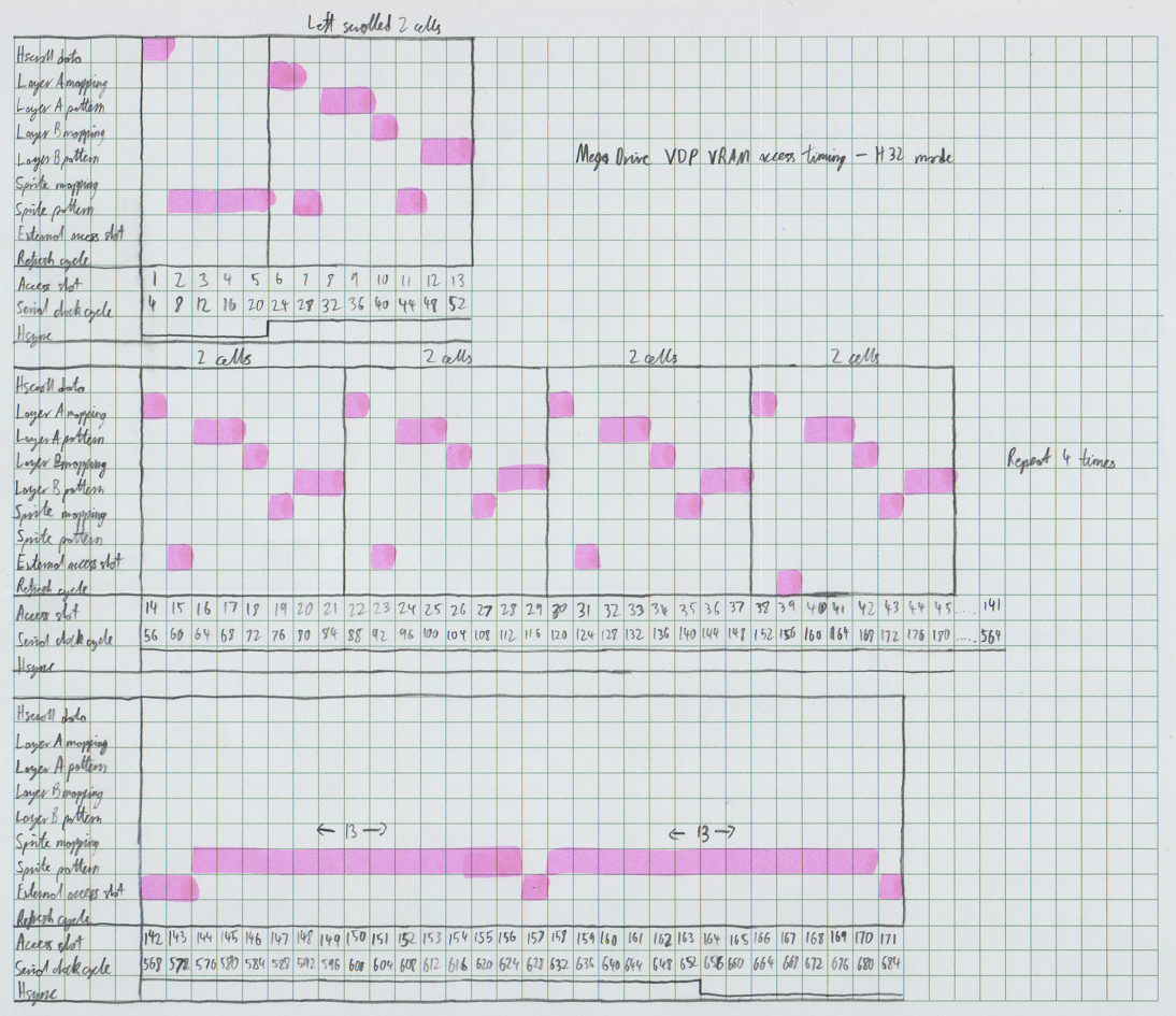
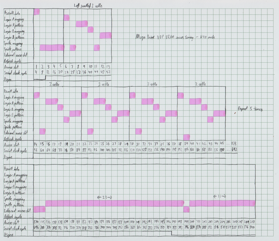
And the source forum post:
Reading and writing VRAM, VSRAM, and CRAM
If you’d like to read or write to VRAM, VSRAM, or CRAM, you need to go through the VDP. VRAM is hooked up to the VDP, not either of the CPUs, and VSRAM and CRAM are internal to the VDP itself.
As discussed above, the VDP is using VRAM, VSRAM and CRAM most of the time in order to draw the screen. The times it’s not are when you can read and write to the various memories from the CPU. On asking for a read, the VDP will use its prefetch mechanism to fill the prefetch latch with the requested data (see below for details). CRAM and VSRAM reads and writes are treated as a word, so only take 1 slot; VRAM reads and writes require 2 slots as they are done 1 byte each.
Wait what’s the FIFO and the prefetch?
The command FIFO is a 4-entry FIFO that buffers commands to write to VRAM. Each time there’s an empty slot, the VDP will write the oldest entry. If the FIFO is full and you try to write a 5th entry, the CPU will be stalled until there is an opportunity to discharge at least one FIFO entry.
However, due to certain design decisions, each FIFO entry requires two VRAM access slots of it is to VRAM, because it can only write one byte at a time - low, then high. CRAM and VSRAM writes are done as full words.
The prefetch is a 1-slot buffer that reads from VRAM. When you set a VRAM address, it is (if possible) immediately prefetched, so that when a read command comes in, the data will be ready.
However, the FIFO gets preference over the prefetches, so if you try to read VRAM while the FIFO is full, the processor will be stalled.
DMA
DMA is actually a pretty simple mechanism. It has 3 “modes”:
- 68k bus -> VRAM, VSRAM, or CRAM
- VRAM -> VRAM
- fill data -> VRAM
The DMA unit, when doing type 1 transfers, uses the FIFO buffer. Depending on the mode, it reads from whichever memory it’s configured to, and puts entries into the FIFO. If the FIFO is full, the DMA unit will pause and wait.
You basically set the destination up as if you were about to do a CPU write, and then trigger the DMA unit. It will then repeatedly read from whichever source, and write it to the data port. This will fill the FIFO buffer with write commands. It then pauses until the FIFO buffer discharges at least once and continues on.
VRAM->VRAM works a bit differently, I’m not exactly sure how, perhaps it uses the prefetch latch. It appears to copy one word at a time.
For fill, the DMA unit will keep writing the last word written to FIFO. When that word is fully written to VRAM, the fill will begin using that value. If you write a new word mid-way through the fill, said write will occur as normal and then be used as the value for the remainder of the fill.
Triggering DMA
For modes 1 and 2, basically anything except fill, DMA starts when you set CD5 (a bit in a control register).
The DMA enable bit in the VDP registers only configures if you can set CD5, as opposed to the general availability of DMA.
For fill mode, you must set it up and then write the value to be used. This will trigger the fill to commence.
TODO: specifics
how to actually start DMAs, etc.